Microfabrication
Protein Crystallography Device Design
Simplifying Protein Crystallography
As an engineer at MiTeGen, I designed and fabricated microfluidic crystal traps in the Cornell NanoScale Facility (CNF) cleanroom, creating bottlenecked channels to capture protein crystals and enable time-resolved fluorescent diffusion measurements under confocal microscopy. I translated CAD designs into functional devices via photolithography, iterating across 70+ SU-8/PDMS prototypes bonded to glass for optical compatibility.
I also designed the experimental protocol and built an automated control system to sequence buffer flushing, crystal loading, and fluorophore delivery; culminating in a published abstract in a local research journal, validating the device and experimental approach.
Highlights:
Abstract Published
70+ Prototypes Built
Automated Test Setup
Partners: MiTeGen, CNF
Role: Engineer
Timeline: May 2022 - May 2024
The Challenge
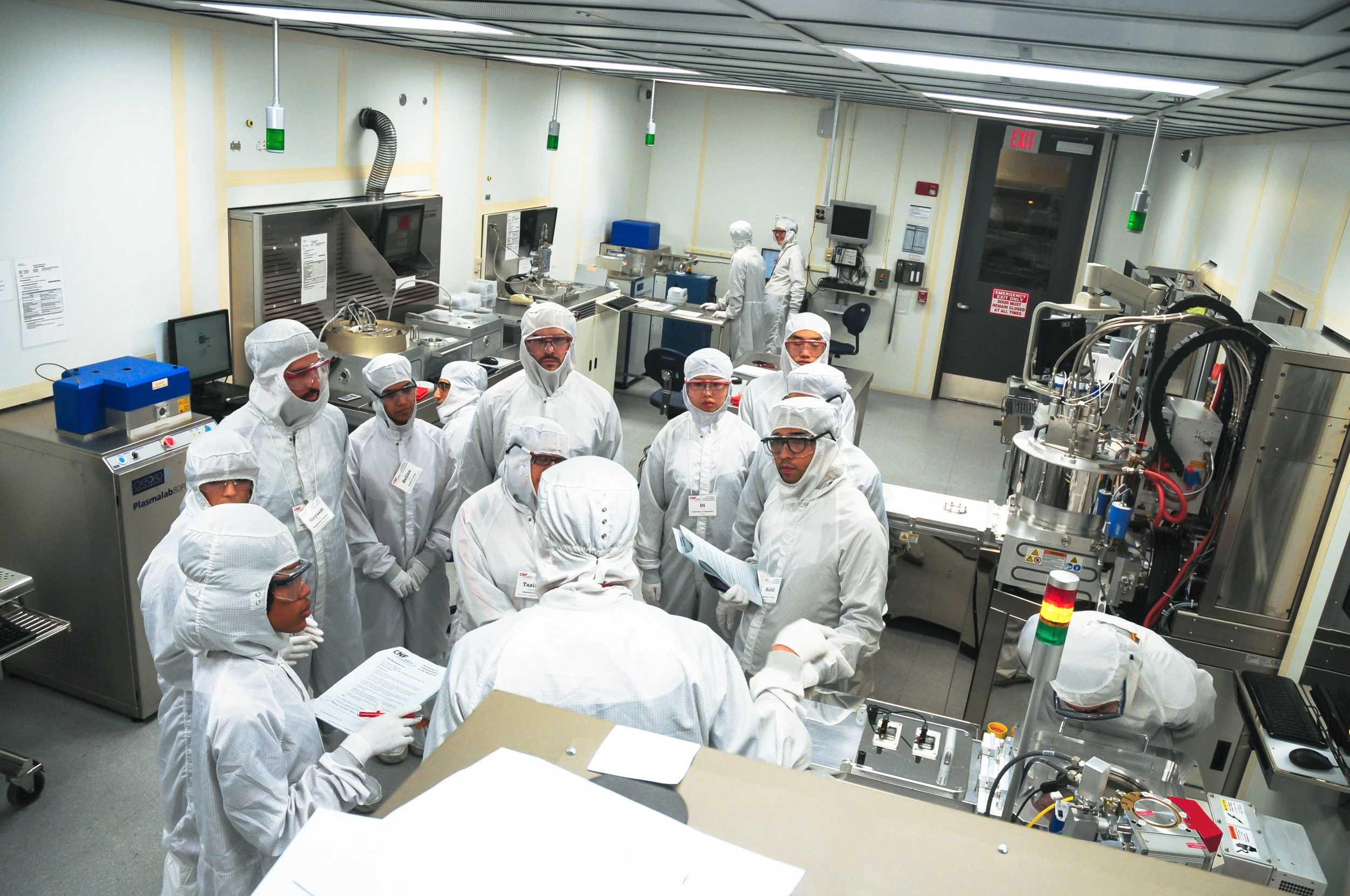
Working in the CNF cleanroom required certification across the full lithography workflow, including the mask writer, SU-8 laminator, contact aligner, and etching tools. The smallest parameter deviations in the process would cascade into device failure, and every new variable required a full resort, making reproducibility the primary goal.
Developing each crystal trap required translating CAD designs into physical devices through a multi-day photolithography pipeline. Wafers were cleaned, laminated with SU-8, exposed through custom-written photomasks, developed to form micron accurate molds, and used as stamps for PDMS casting and glass bonding. Each step introduced opportunities for defects, so process control and documentation became just as important as the design itself.
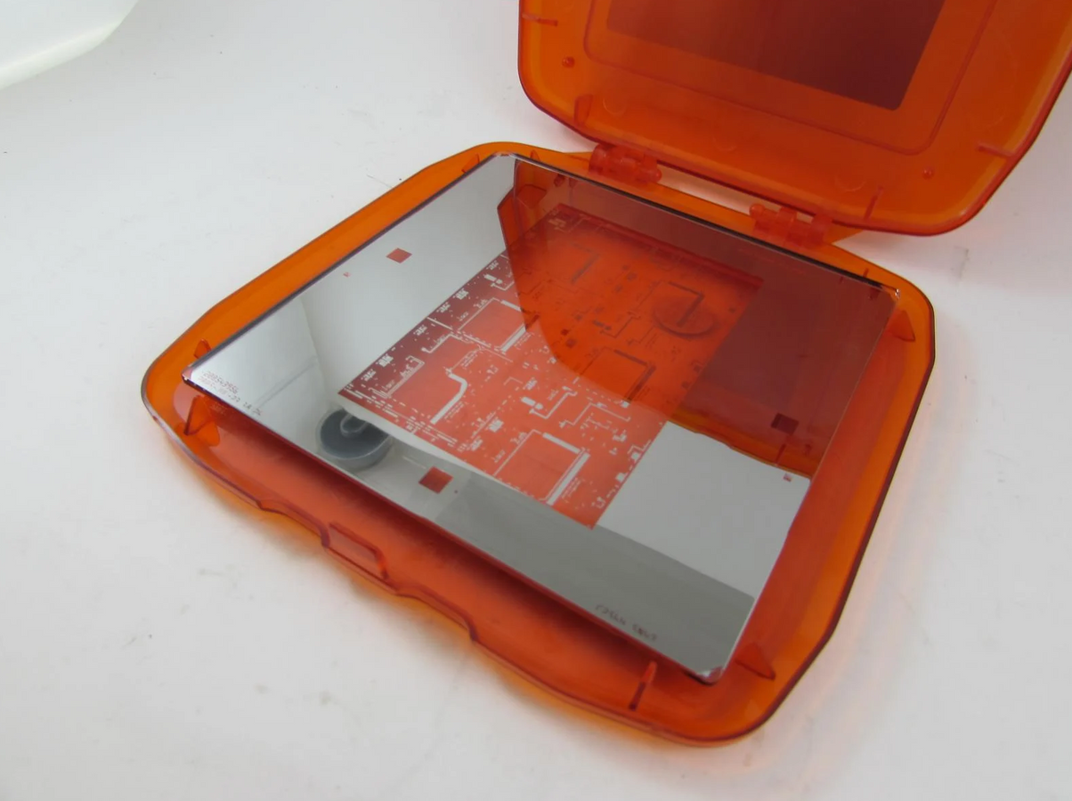
Sample (not mine) etched photomask used to obscure part of a silicon wafer, so only the desired design is exposed.
The trap design evolved through rapid iteration. Early devices were too thick and difficult to integrate with microscopy setups. Thinning the PDMS improved usability, but led to channel rupture. Simplifying from three inlets to one reduced internal pressure gradients but increased stability demands on each channel . . .
Balancing fluid dynamics, material properties, and cost became the core challenge. While each silicon wafer is reusable (so long as the SU-8 is intact), the traps are single use, meaning increasing PDMS crosslinking improved channel stability, but increased brittleness and cost - forcing careful tradeoffs between robustness, manufacturability, and experimental usability.
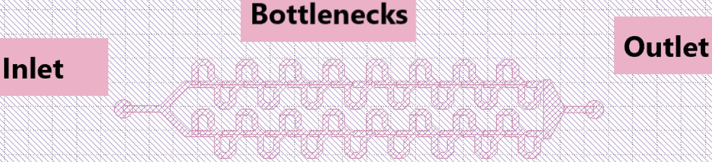
Labelled components of final trap design
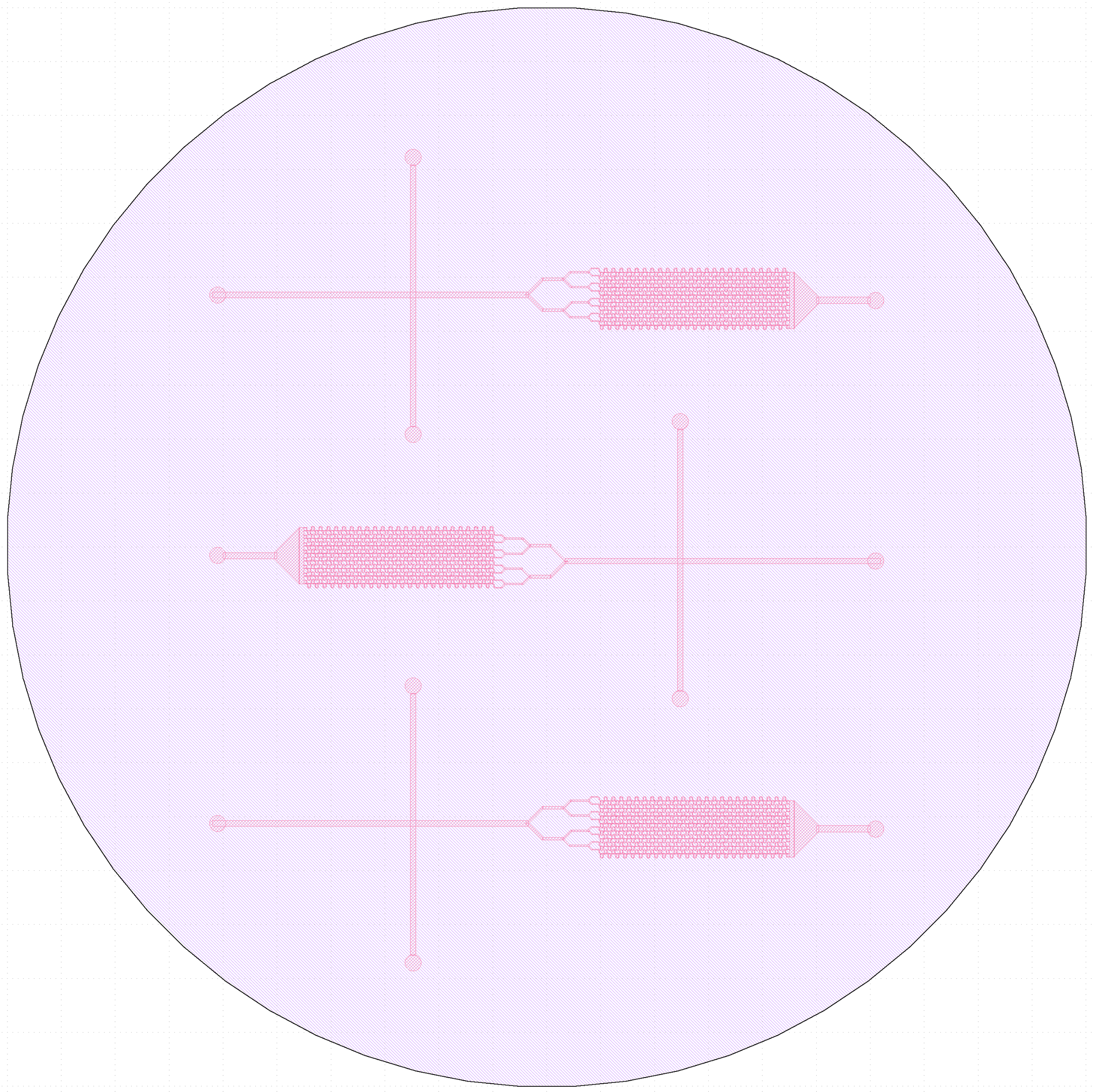
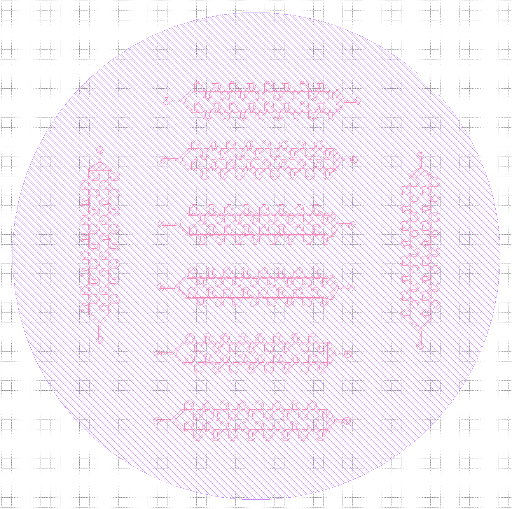
Original (3-inlet) trap design vs final (single inlet) design.
The Solution
With the design finalized, I built a structured workflow to test inlet geometry, priming, flow rates, and crystal loading, establishing a repeatable baseline and reducing confounding failures.
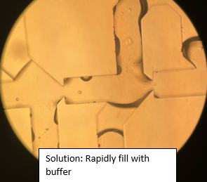
Standardizing priming and loading improved trap reliability. Rapid buffer priming prevented channel bypassing, while controlled injection angles minimized PDMS damage and leakage, stabilizing flow and enabling consistent crystal capture in bottleneck regions.
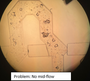
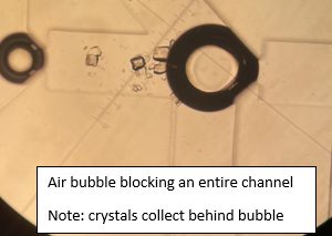
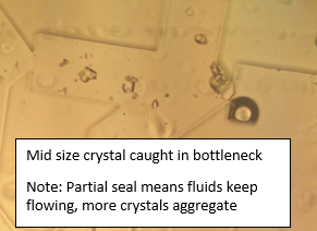
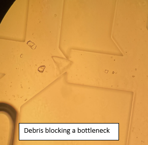
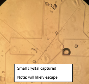
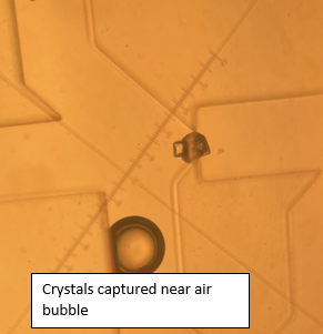
Iterative testing revealed key failure modes - air bubbles, debris-blocked bottlenecks, and poor midline flow, which were mitigated through process controls like pre-priming tubing and forcing full-channel wetting.
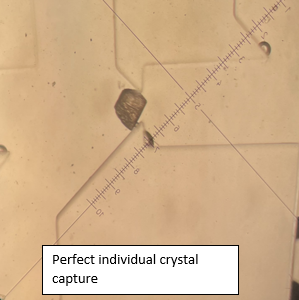
The final design demonstrated size-selective trapping, with channel thickness governing whether crystals passed through or were captured, simplifying tuning for future use cases.
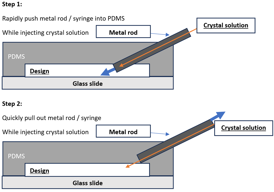
Visualization of solution injection.
The finalized workflow improved experimental efficiency and reproducibility by minimizing inlet damage, reducing fluid use, and defining reuse limits for PDMS traps; turning a fragile prototype into a practical, repeatable platform for high-throughput crystal handling and fluorescence analysis.
Finally, I built an automated control system using an Arduino, actuator, SPDT switching, and a syringe pump to sequence buffer priming, crystal loading, and fluorophore delivery. This ensures only the desired solution is being introduced at a constant flow rate, standardizing conditions and reducing user variability across devices.
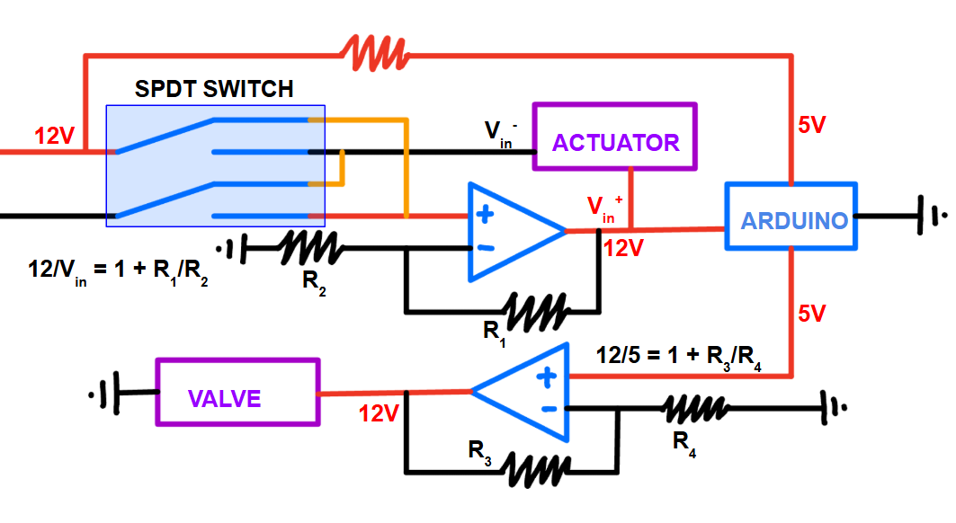
Control system circuit design with labelled specifications.